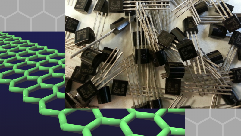
As electronic gadgets dominate many aspects of our lives, smaller devices that pack more functionality and consume lower power are increasingly becoming popular. Transistors—one of the basic building blocks of these devices—dictate their size, speed, efficiency and battery life. In a recent study, Ms Poonam Jangid, Mr Dawuth Pathan and Prof.Anil Kottantharayil from the Indian Institute of Technology Bombay (IIT Bombay) have developed a technique to fabricate graphene transistors as small as 20 nanometers wide (5000 times smaller than the thickness of a sheet of paper). These graphene transistors consume less power in the standby state and can facilitate faster circuit operations.
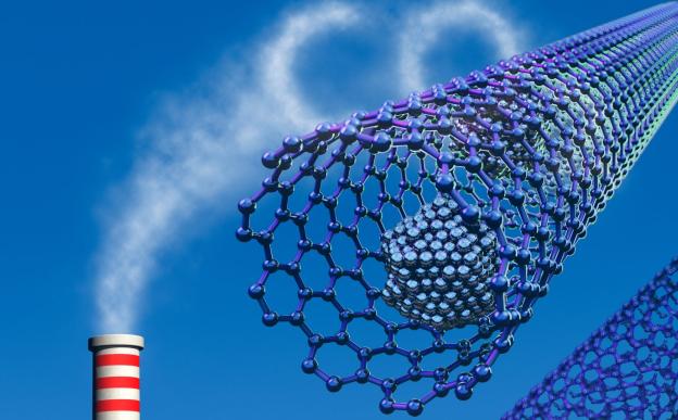
Silicon and similar semiconductor materials have been traditionally used to build transistors. However, there are significant challenges to making smaller but faster silicon transistors. An alternative is graphene, which is a crystalline form of carbon that is made up of a single layer of carbon atoms. In its pure form, graphene is a conductor. But, by altering its structure, it can be turned into a semiconductor, making it an ideal candidate for next-generation transistors and other electronic devices.
Graphene nanoribbons are strips of graphene made by creating parallel channels on its surface by removing some carbon atoms. Previous studies have shown that the conductivity of graphene can be controlled by changing the width and structure of the edge of the channel; the narrower the width of the ribbon, lesser is the conductivity. “Compared to silicon transistors, graphene transistors can be 100 times faster," says Prof. Kottantharayil.
So far, graphene nanoribbons are synthesised either through chemical processes or by etching on graphene films using nanocrystals of metals like nickel, copper or iron. However, neither chemical synthesis nor any known method of etching yields graphene nanoribbons with a smooth and desirable edge structure. In this study, published in the journal Carbon, the researchers have fabricated graphene nanoribbons by etching graphene films using platinum nanocrystals. Since platinum is a nearly-inert material and is a useful chemical catalyst, it yielded good quality graphene nanoribbons, with a width of 10-20 nm and smooth edges. The process was carried out at a temperature of about 1000oC in the presence of a mixture of hydrogen and argon gas.
Transistors act as switches that allow current to flow when they are turned on and stop it when they are switched off. However, in practice, a small, negligible current, called leakage current (IOFF), flows even when the transistor is off. It is because of this leakage current that electronic devices consume battery power even in the standby mode. Ideally, an efficient transistor would aim at having the lowest possible value for the leakage current. A higher value of the current passing through a transistor when it's on (ION) indicates that the device has a higher conductivity, and can be turned on and off faster.
“ION/IOFF is a figure of merit for the switching efficacy of transistors. High ION results in faster circuits and low IOFF is desirable for low standby power,” explains Prof Kottantharayil.
The new graphene transistor designed by the researchers showed a high ION/IOFF ratio of 600 at room temperature and a high conductivity compared to not only traditional transistors but also to graphene nanoribbon transistors made by other methods. Although graphene nanoribbon transistors fabricated using nickel nanocrystal-based etching have a higher ION/IOFF ratio of 5000 at room temperature, they have very low conductivity, which may tend to heat the device, reducing its efficiency.
Although the findings of the study are exciting, graphene nanoribbon transistors are still far away from reality. “To be used in nanoscale circuits, it is essential to fabricate graphene nanoribbons on a large scale with lesser defects. Graphene nanoribbons are at least ten years, if not farther, from widespread applications,” says Prof Kottantharayil.
A major drawback of synthesising graphene nanoribbons by etching is that they contain many defects. Hence, to produce nanoribbons on a large scale, non-etching based techniques need to be developed.
“Some possible research direction include directed movement of catalyst nanoparticles that are deposited or grown at specific locations of interest. Some of the techniques used in our research along with etching based techniques could be interesting to study,” Prof. Kottantharayil signs off.


