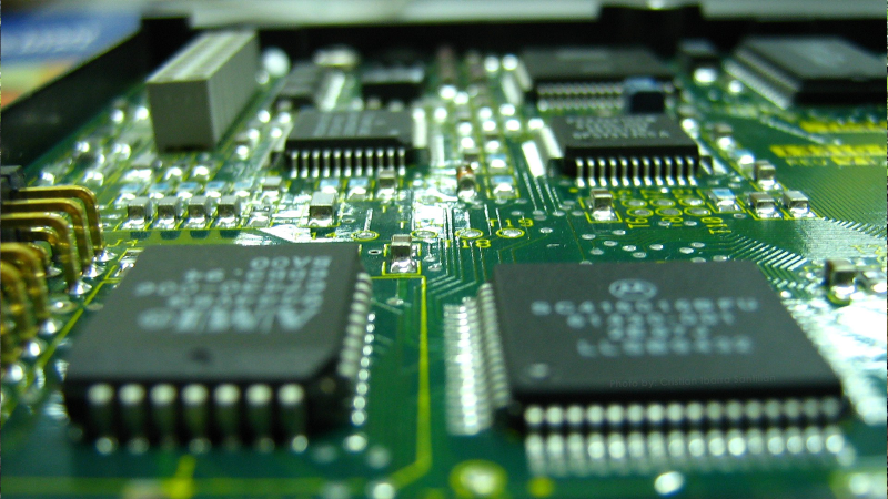
Silicon chip-based electronic circuits, the ones used in mobile phones, laptops, wifi routers and of late in smart devices, mostly have logic circuits. Some also need memory elements to hold data, such as device identity or security key. A security key is essential to keep data safe, whether for financial transactions, subscriptions such as Netflix or our personal data.
Prof Udayan Ganguly at the Department of Electrical Engineering, IIT Bombay and his team are leading an effort to demonstrate indigenous semiconductor memory for secure applications. They have the credit for making the first indigenous memory technology translated from Lab to Fab.
In partnership with Semiconductor Labs, Chandigarh, Prof Ganguly, and his team have demonstrated a one-time programmable memory technology. It can be used in secure memories, hardware encryption and artificial intelligence. The work was presented at the IIT R&D Fair 2021 by Kumar Priyadasrhi and Udayan Ganguly from IIT Bombay.
Today, memory innovation is driving semiconductors. Data encryption is needed to protect your critical private information every time you upload your pictures and videos onto the cloud. Artificial intelligence provides a new future that opens vistas of amazing possibilities. So commercial memory needs are driving business and innovation for memory technologies globally.
Strategic needs for India stress having indigenous memory extremely critical. We need to secure identities for e-commerce, data security to store information in the cloud and ultimately, artificial intelligence that will make sense of it all. With secure memory being so critical, the question is, can India build her own memory technology?
The team proposed a nanoscale structure for a memory cell in this context. A very thin layer of Silicon Oxide is sandwiched between two metal layers. The silicon oxide layer is just 2.5 nanometers, only 15 atoms thick! The structure forms a nanocapacitor and does not let electrical current pass. This pristine or undisturbed silicon oxide thus forms the state zero.
Prof Ganguly explains how One-Time-Programmable (OTP) memory is done, “If we introduce the equivalent of lightning inside this capacitor, the insulator breaks down and starts passing electric current. In this broken-down insulator, the line inside the solid material is retained permanently and allows the passage of current forever. Thus, we have created two states, the pristine state that passes no current and the broken-down state that passes high current. This programming can be done once, but it can be read many times till perpetuity.”
Prof Ganguly notes that the research began in 2015 with a PhD thesis that detailed the method of making OTP memory. This idea was placed in front of SCL Engineers, who realised that this could be placed into their fabrication line. IIT Bombay and SCL collaborated, and by 2019, they were working vigorously as a team to scale the IIT Bombay technology to 200-millimetre wafers for production. By 2021, they had created a set of specifications to enable an 8-bit calibration or trimming application. They have recently demonstrated a 97 per cent yield in the Fab.
The next step is to enable the manufacturing of products based on these technologies. Collaboration between IIT Bombay, a nano fab facility and an academic institution, and manufacturing partners, SCL Chandigarh fructified, thus resulting in the lab outcomes reaching all the way to the fab towards a manufacturing innovation.
From 2015 till today, technology development has been possible with funding from different agencies, including the Department of Science and Technology, the Ministry of Electronics and Information Technology, and the Office of the Principal Scientific Adviser to the Government of India. It's also been helped along by fantastic collaborators from IIT Delhi, SETS Chennai and DRDO, enabling different applications or serving with their expertise to enable various capabilities.
After going through several manufacturing readiness levels, the technology is ready for production. The engineers identified basic manufacturing implications, all the way down to eight steps, where the pilot line capability is. They demonstrated a low rate of production. Now the capability is in place for the full rate of production.
Now that this technology has been established, there is a reasonably rich application roadmap. There is a veritable roadmap. The primary application is the trimming or calibration, which will be able to upload small calibration constants to correct any shifts in analogue design. Other applications include hardware encryption that enables authentication and secure data, secure memory that enables memories to have encrypted data, radiation hard memory for space applications and neural network chips based on OTP technology.
After achieving the technology milestone, the logical next step is to put out applications in the strategic and commercial space. It is a journey that has to go out of the academic space into the commercial space. A deep-tech startup called Numelo Technologies (neural networks, memory and logic technologies) was incubated in 2021 to venture into commercial space. While this journey is daunting, they have wonderful partnerships with SCL, DRDO, and some foreign foundries. Partnerships with other academic and research agencies are also thriving.
The OTP memory technology has a total addressable market size estimated at the US $140 million. Significant applications are government identifications like e-passports, consuming about 40 million chips per year. Mobile phones with near field communication and touchless, cashless transactions can also use OPT memory. Then there are secure NaVIC ICs, GPS, and embedded systems for strategic applications. And finally, there is this whole vista of edge and autonomous security AI chips for strategic applications. So this is indeed a large market for a new technology based on a secure memory. India-owned technology and design enable and ensure national security.
Editor's Note: The title was edited due to a typo. The mistake is regretted.


