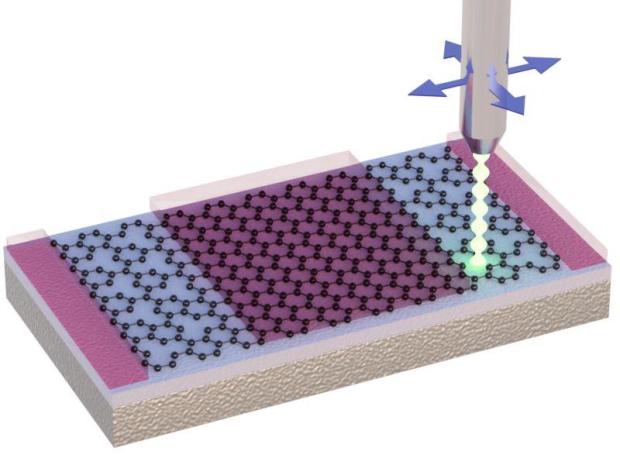
High-energy electron bombardment. Photo: Mayank Shrivastava, DESE
In a major breakthrough in the field of graphene based electronics, researchers from the Indian Institute of Science, Bangalore, have shown a big jump in understanding the quantum nature of graphene’s interface with outside world. The research team lead by Prof. Mayank Shrivastava (Department of Electronic Systems Engineering), studied how the overlap of atomic orbitals between Carbon and metal atoms affects the graphene-metal interface. The study has enabled them to invent novel techniques to engineer graphene contact that has the lowest recorded resistance to the external world. Their discovery and subsequent invention, while breaking several records – including the one from IBM’s research centre in T. J. Watson, USA – has eventually allowed achieving the highest transistor performance. This work, which is co-authored by PhD student Adil Meersha and co-investigators Prof. Srinivasan Raghavan and Prof. Navakanta Bhat is showcased at International Electron Device Meeting (IEDM), the world’s most competitive platform in the field of electron devices, which mostly showcases technology and fundamental breakthroughs in the field.
Ever since its discovery in 2004, graphene – a two dimensional, single atom thick layer of Carbon atoms, has gained prominence in the semiconductor and electronics industry due to its exceptional properties. But, a phenomenon called contact resistance, the resistance offered at the point of contact between the metal and graphene, poses a challenge. “The problem of the contact resistance is, even today, considered as one of the most fundamental bottle-neck in realizing this technology. Until we are able to interface graphene with the outside world with very little resistance, we will not be able to squeeze out its projected performance”, says Prof. Shrivastava on the need to solve this bottle-neck.
Scientists all over the world had believed that the lowest limit on contact resistance was already achieved and not much can be achieved further. This research has now debunked the belief by exploring the theoretical aspects at a much deeper level involving quantum chemistry. In a previous study, Prof. Shrivastava’s team had established a link between unfilled electron orbitals around the carbon nucleus, its hybridization or atomic overlap with metal atom and resultant electron transport from metal to graphene. “Atoms are made of a nucleus surrounded by electrons arranged in several orbits called 1s, 2s, 2p, 3s, 3p, 3d and so on, which have unique shapes depicting the region in which probability of finding the electron is maximum. Each orbit can accommodate a fixed number of electrons and when they are in the vicinity of orbits of another atom, they tend to reshape by sharing electrons – called hybridization, which we engineered and formed bonding channels” – explains Prof. Shrivastava.
In the case of graphene, shared electrons of the neighbouring Carbon atoms fill up the unfilled electron orbits through the process called hybridization. By knocking off some of the shared electrons, the unfilled p orbitals can be filled by electrons in a metal with similar unfilled s and p orbitals. “We were trying to see if defects in graphene could affect contact resistance, from a theoretical aspect. We found that by knocking off electrons from some Carbon atoms, an unfilled “p” orbit becomes available, which allows for a better bonding with the metal through bonding channels. These channels, in turn, reduce the contact resistance”, explains Prof. Shrivastava. The researchers found that focussing a beam of electrons on graphene or bombarding it with Argon or Oxygen ions forms the required defects. This would enable hybridizing metal atoms with graphene.
This discovery could herald a new era in utilizing the underutilized terahertz frequency range, band within the electromagnetic spectrum, lying between microwave and infrared. Due to its safe, non-destructive and non-invasive properties, the terahertz frequency could be used for applications as wide ranging as high altitude communication and faster wireless communication to surveillance and security. “Graphene transistors are expected to be the enabler of THz technology– a billion dollar high end application market, which is still untouched due to unavailability of electronics to control and manipulate THz radiation. With this breakthrough, we foresee commercialization of THz graphene technology in the near future, which was earlier projected to be around 2022”, remarks Prof. Shrivastava.
This study also reflects how exploring theoretical and fundamental concepts of a problem, which many consider an impasse, could lead to technological innovation. The researchers successfully predicted the actual cause behind contact resistance offered by graphene and proceeded to solve it at an atomic level. The process leading up to the design could also set a precedent, where experimentalists opt for a theoretical basis to solve a problem, rather than the usual trial and error method.


