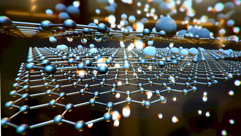
Graphene, a sheet-like form of carbon, has been hailed as a wonder material owing to its many promising applications in electronics, drug delivery and more. In a recent study, a team of scientists from India and the USA, led by Prof Srinivasan Raghavan and Prof Rudra Pratap from the Indian Institute of Science (IISc), Bengaluru, has paved the way for new applications of graphene by intentionally varying the defects formed during its production.
Graphene is commonly produced using a technique called chemical vapour deposition (CVD) in which metals such as copper and platinum are exposed to hydrocarbons like ethane and methane. These hydrocarbons decompose and deposit on the metal substrate, forming a film. The graphene produced by this method inevitably develops defects called grain boundaries, in its crystal structure. Changes in the grain boundaries change the mechanical, electrical and other properties of the material. In the current study, done as part of Mr Krishna Bharadwaj’s PhD, the researchers have come up with a novel mechanism to create and heal the defects in the grain boundaries of graphene in a reversible manner. In doing so they have created graphene with one of the highest reported room temperature electronic mobilities till date.
“This work has the potential to find use in a broad spectrum of industries. It could range from terahertz electronics, which benefit from the high electron mobility in graphene, to even packaging industries which require near-zero permeability of water attainable by graphene layer coating,” says Prof Srinivasan Raghavan.
The study, published in the journal Nature Communications, was funded by the Department of Science and Technology and the Thematic Unit of Excellence for Nano Science and Technology project.
The researchers studied graphene samples produced by CVD on a copper surface in different ways. The first sample was grown by keeping all the reaction conditions for the growth of graphene a constant. After some time, they observed a completely covered film of graphene on the copper sheet using a scanning electron microscope. They measured the changes in electrical properties, such as charge mobility and sheet resistance, of this film and compared them to the values for the other three samples.
In the second sample, the researchers initially had the conditions that drive the growth of graphene a constant until the copper surface was covered entirely with graphene film. Then they raised a reaction condition called the carbon potential to a slightly higher value. The values of the electrical properties then showed an increase over the first sample.
The third sample was initially grown like the second one. But, after a higher value of carbon potential was reached, it was lowered back again to the initial value. The electrical properties initially increased and then decreased, tracing back the previous rise, demonstrating reversible behaviour.
Any chemical reaction can be influenced by two types of factors — kinetic factors, which are related to the speed of the reaction, and thermodynamic factors related to its energy requirements. Depending on which of the two plays a significant role, a reaction can be called 'kinetically controlled' or 'thermodynamically controlled' reaction. The reversible nature of the phenomena confirmed it was thermodynamically controlled in the case of graphene growth.
“The growth of atomic layers is not as easy as it seems,” said Prof. Raghavan. “A thermodynamic lever improves our capability to control growth,” he added.
Further, the researchers made a replica of the graphene structures on a germanium film to visualise the defects in the graphene film. To do this, they allowed water to pass through the graphene film by placing a water droplet on top. Since water can only permeate through the defective grain boundaries and not any other part of the graphene layer, using optical and atomic force microscopy, they observed the impression of water along the grain boundaries. They found that most of the defects of the graphene layer lie in the grain boundaries, confirming that the changes in the electrical values are occurring due to the decrease and increase in the grain boundary defects.
“If graphene could make paper impermeable to water, then it can be a substitute for plastic and hence could solve many of the garbage problems that we are facing today. That is a challenging problem, and we are working on it,” adds Dr Srinivasan Raghavan as an exciting problem close to his heart.
This article has been run past the researchers, whose work is covered, to ensure accuracy.
